🔍 TL;DR – PCB Impedance Control Begins with Stackup Collaboration
- PCB impedance control starts upstream — with the stackup.
- Your design tool is helpful, but it can’t build your board.
- Real stackup collaboration = faster builds, better margins, and fewer surprises.
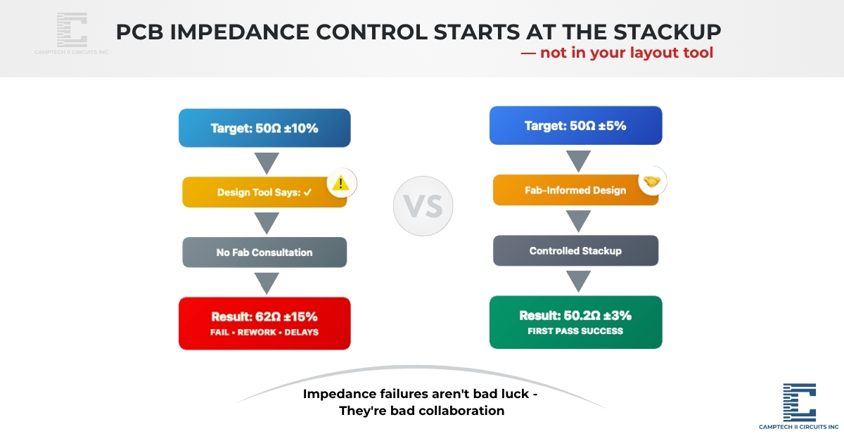
Most PCB engineers assume impedance is under control the moment layout is done. The tool says 50Ω ±10%, and you’re good to go—right?
But then the board comes back at 62Ω ±15%.
Now you’re over budget, behind schedule, and trying to explain why the re-spin happened.
Impedance failures aren’t bad luck. They’re bad collaboration.
And most of them start with one thing: assuming your layout tool can handle stackup reality on its own.
🚧 The Hidden Cost of Stackup Assumptions
Impedance problems don’t usually come from poor routing.
They come from mismatches between your design assumptions and fab realities.
Here’s where it breaks:
- Your tool’s dielectric model isn’t based on the fab’s actual material set.
- Layer naming like “Top” or “Signal1” causes trace misalignment.
- “Standard copper” = five emails and three clarifications.
- No pre-fab check = surprise impedance failure after you’ve paid for the build.
These aren’t design flaws. They’re communication breakdowns.
🧠 Why Layout Tools Aren’t Enough
Your EDA tool simulates in ideal conditions. But your fabricator builds in the real world—with material tolerances, etching variability, copper distribution shifts, and process dependencies.
Here’s what most layout tools don’t account for:
- Real dielectric stackups and pressout thickness
- Actual copper weight and plating variation
- Etch-back differences on signal layers
- Prepreg choices and resin content by lot
- In-process variability across panel builds
PCB impedance is not just a routing spec — it’s a fabrication outcome.
✅ What Fab-Controlled Stackups Do Differently
When you design using actual stackup data provided by your fabricator, you shift from simulation to control.
| Scenario | Tool-Only Design | Fab-Informed Design |
|---|---|---|
| Impedance Target | 50Ω ±10% | 50Ω ±5% |
| Stackup Input | Tool defaults | Actual material & copper spec |
| Layer Naming | Internal guesswork | Coordinated with fab |
| Result | 62Ω ±15% — Fail | 50.2Ω ±3% — First-pass success |
🧰 How to Prevent Impedance-Related Rework
You don’t need a new tool—you need a new approach.
Here’s what actually works:
- Share real stackup data before layout
Don’t rely on outdated templates or IPC defaults - Call out impedance + trace geometry in context
Specify where and why you need it - Collaborate early with your PCB fabricator
Don’t wait until the files are sent - TDR-verify when impedance really matters
Especially for RF or high-speed lines - Treat DFM like part of the spec
Not a suggestion or afterthought
At Camptech Circuits, we help engineers eliminate rework before layout even begins. Stackup reviews are part of the process—at no cost.
💡 Want First-Pass Success?
📩 Send us your files for a free stackup consultation.
We’ll flag any impedance risks and help you hit spec before it costs you.


